How to Design an SPI Master Controller in Verilog RTL
Learn how to design an SPI Master Controller in synthesizable Verilog RTL, integrate APB, implement SPI timing, verify the design, debug synthesis warnings, and analyze timing, area and power.
What are we building?
What happens when a processor wants to send one byte to an SPI peripheral?
Somewhere between an APB write and the first SCLK edge, that byte has to become a precisely timed stream of serial bits.
In this guide, we will build that path step by step — starting with SPI fundamentals, moving through APB-controlled register access and modular Verilog RTL, and finally taking the design through simulation, lint, synthesis, timing, area and power analysis.
The goal is not only to make an SPI waveform appear.
The goal is to understand what the RTL is doing, why it works, and what happens to it after synthesis.
What you will build
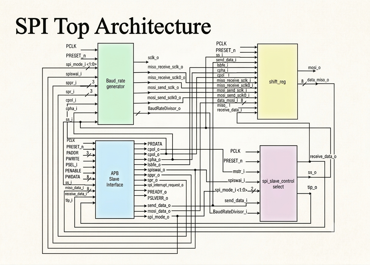
The final controller is organized into four functional RTL blocks plus a top-level integration module:
| RTL block | Main responsibility |
|---|---|
APB_SLAVE_INTERFACE.v |
APB transactions, configuration/status/data registers and interrupt logic |
BAUD_GENERATOR.v |
Programmable SPI clock generation and timing events |
SPI_SHIFT_REGISTER.v |
Serial TX/RX datapath |
SPI_SLAVE_CONTROL_SELECT.v |
Slave-select, transfer counting and completion control |
SPI_TOP.v |
Top-level integration |
Current implementation: WIDTH = 8
What you will learn
By the end of the guide, you should be able to follow:
- How SPI communication works
- What CPOL and CPHA actually control
- How an APB transaction can configure and drive an SPI peripheral
- How to break a controller into synthesizable RTL modules
- How a programmable baud generator produces SCLK timing
- How a shift register performs SPI transmit and receive operations
- How to construct and read a verification waveform
- What RTL lint and
check_designare looking for - What synthesis does to RTL
- How to interpret timing, area and power reports
- How to investigate a synthesis warning instead of assuming the RTL is broken
- What a synthesized netlist represents
1. SPI Fundamentals
What is SPI?
Picture two chips that need to exchange data — but instead of shouting numbers across a room, they agree on something far more disciplined: one of them keeps a steady beat, and every bit gets exchanged on that beat. That is the basic idea behind SPI (Serial Peripheral Interface), a synchronous serial communication protocol.
One device acts as the master. It generates the clock (SCLK) and decides when a transfer starts. A slave is selected using a dedicated Slave Select (SS) or Chip Select (CS) signal.
SPI intentionally keeps the interface simple. It normally uses a clock, one line from master to slave (MOSI), one line from slave to master (MISO), and a select line.
In short: SPI trades a small, simple interface for a clean clocked data-transfer mechanism.
SPI signals
| Signal | Direction from master perspective | Purpose |
|---|---|---|
SCLK |
Output | Serial clock |
MOSI |
Output | Master Out, Slave In |
MISO |
Input | Master In, Slave Out |
SS/CS |
Output | Selects the target slave |
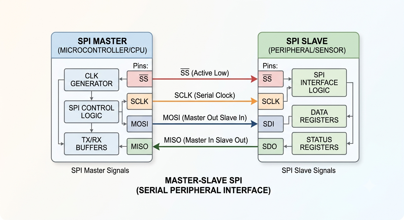
Full-Duplex Transfer: Talking and Listening at the Same Time
Here’s a useful mental model: SPI can transmit and receive on the same clocked transfer. While the master is sending a bit over MOSI, it can simultaneously sample a bit coming back over MISO.
The Shift Register block is where this dual activity happens. One path shifts transmit data toward MOSI, while another accumulates bits sampled from MISO.
Watching It Happen, Bit by Bit
Let’s make this concrete with two 8-bit shift registers — Tx_shift_reg and Rx_shift_reg.
Sending: Tx_shift_reg holds 178 (10110010). The representative example below assumes MSB-first transmission and shows the bit sequence being driven:
| SCLK edge | 1 | 2 | 3 | 4 | 5 | 6 | 7 | 8 |
|---|---|---|---|---|---|---|---|---|
| MOSI | 1 | 0 | 1 | 1 | 0 | 0 | 1 | 0 |
Receiving: At the same time, Rx_shift_reg samples the slave’s MISO bits. For the representative waveform used later, the received byte is 109 (01101101):
| SCLK edge | 1 | 2 | 3 | 4 | 5 | 6 | 7 | 8 |
|---|---|---|---|---|---|---|---|---|
| MISO | 0 | 1 | 1 | 0 | 1 | 1 | 0 | 1 |
The important point is that transmit and receive are part of the same SPI clocked transfer.
In short: full-duplex SPI uses one shared clock to coordinate simultaneous transmit and receive datapaths.
2. SPI Clocking: CPOL and CPHA
CPOL
CPOL (Clock Polarity) determines the idle level of SCLK.
CPOL = 0: SCLK idles lowCPOL = 1: SCLK idles high
CPHA
CPHA (Clock Phase) determines which active edge is used for sampling relative to the SPI transfer’s first and second active edges.
CPHA = 0: sample on the first active edgeCPHA = 1: sample on the second active edge
The four standard mode combinations
| SPI mode | CPOL | CPHA |
|---|---|---|
| Mode 0 | 0 | 0 |
| Mode 1 | 0 | 1 |
| Mode 2 | 1 | 0 |
| Mode 3 | 1 | 1 |
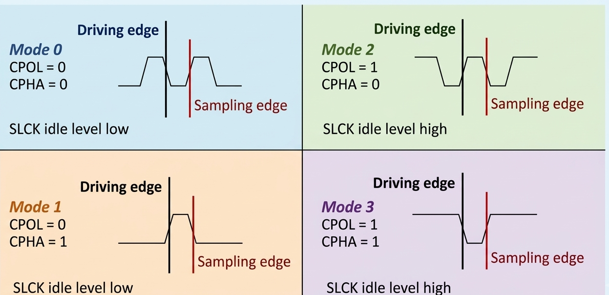
How CPOL and CPHA are used in this RTL
The exact edge-event behavior is implemented by the combination of BAUD_GENERATOR.v and SPI_SHIFT_REGISTER.v.
In the current RTL, the CPOL/CPHA combination selects which generated timing event is used for receiving and which is used for sending. When CPOL and CPHA are equal, the receive/send event assignment is different from the case where they are unequal.
The important design idea is that the transmit and receive events are separated in time so the driven data has time to become stable before it is sampled.
3. Why APB Is Connected to SPI
Picture a busy office. Inside, the processor speaks a structured bus language with addresses and read/write transactions. Outside, an SPI peripheral communicates using clocked serial bits.
These two interfaces serve different purposes. APB gives software a convenient way to configure and control a peripheral. SPI provides the actual serial communication link.
When the processor wants to configure the SPI clock speed, send a byte, or read received data, it writes to or reads from registers exposed by the APB slave interface.
flowchart TD
    A[APB Master] --> B[APB Slave Interface]
    B --> C[SPI Controller]
    C --> D[SCLK]
    C --> E[MOSI]
    C --> F[MISO]
    C --> G[SS]
The APB slave interface is therefore the bridge between software-visible control and the SPI datapath.
4. APB Fundamentals
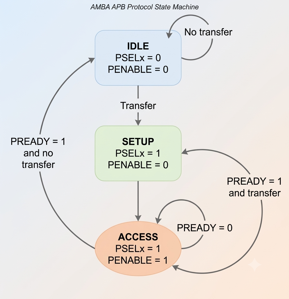
The Basic APB Transfer
Every APB transaction follows a simple phase sequence:
flowchart LR
    A[IDLE] --> B[SETUP]
    B --> C[ENABLE]
    C --> A
IDLE means no APB transfer is currently taking place.
During SETUP, the master selects the peripheral and presents the address and transaction information.
During ENABLE, the transfer is completed. In this implementation, PREADY_O is asserted during the ENABLE state, so the controller completes the transfer without adding wait states.
Meet the Signals
You do not need the entire APB specification to understand this project. These signals are the important ones here:
| Signal | Purpose |
|---|---|
PSEL |
Selects the APB slave |
PENABLE |
Marks the ENABLE phase |
PWRITE |
Selects write (1) or read (0) |
PADDR |
Selects the target register |
PWDATA |
Write data from the APB master |
PRDATA |
Read data returned by the APB slave |
PREADY |
Indicates that the transfer can complete |
PSLVERR |
Reports the implemented APB error condition |
Together, these signals define the software-facing transaction side of the controller.
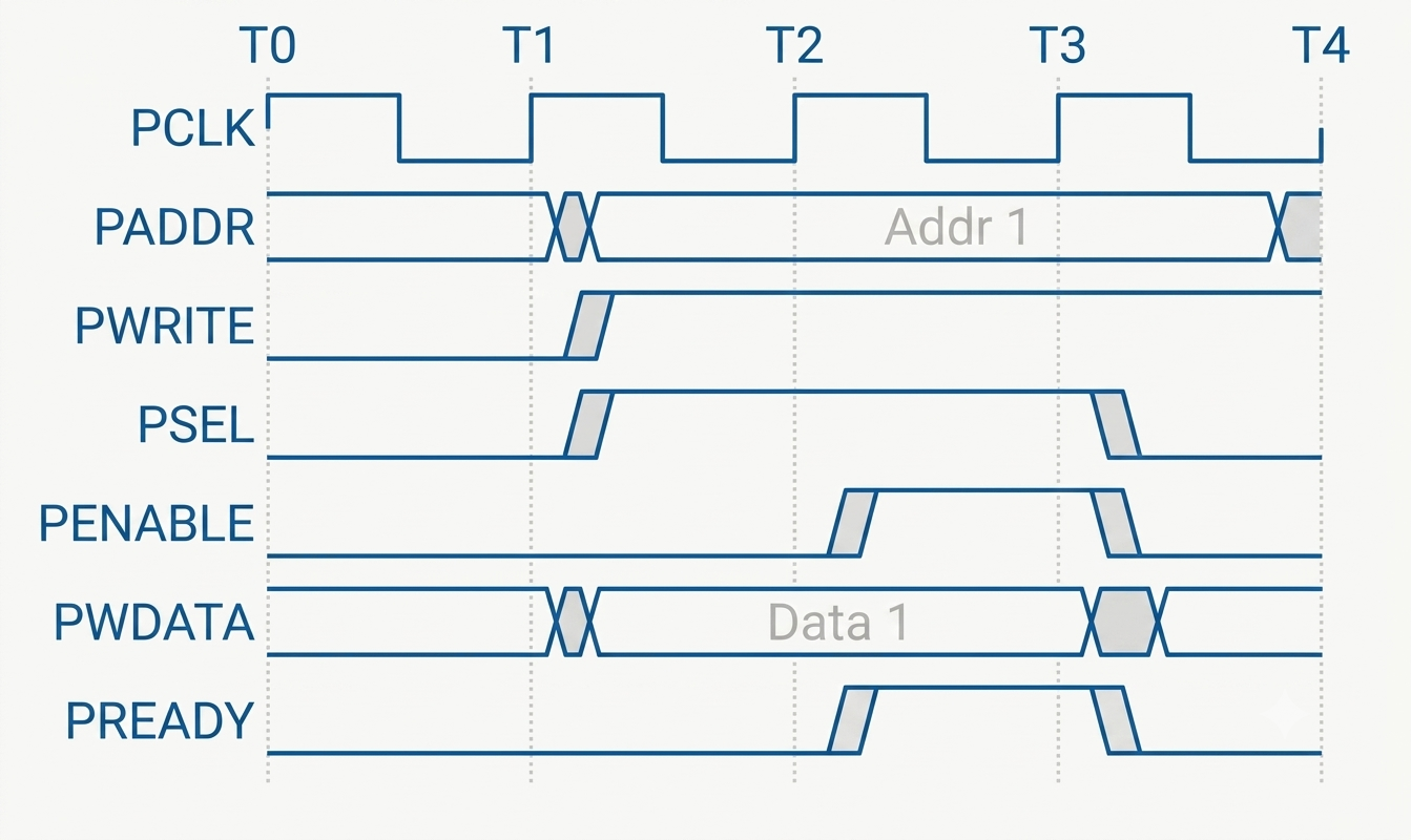
APB state machine
5. Designing the Register Interface
The controller exposes configuration, status and data through registers.
Register map
| Register | Address | Purpose |
|---|---|---|
CR1 |
0 |
SPI control/configuration |
CR2 |
1 |
Additional SPI control |
BR |
2 |
Baud-rate configuration |
STATUS |
3 |
SPI status |
DR |
5 |
Transmit/receive data |
Why register-based control?
Imagine handing the SPI peripheral a to-do list instead of shouting instructions at it one at a time. The registers provide a shared software-visible interface where the processor specifies what to send, how the SPI should operate, and what status it wants to inspect.
The current implementation uses five register locations, each with a specific job.
| Register | The question it answers |
|---|---|
| Control Register 1(CR1) | What SPI mode and bit order should be used? This includes fields such as MSTR, CPOL, CPHA and LSBFE. |
| Control Register 2(CR2) | Should the SPI wait according to SPISWAI, and how should additional control such as mode-fault-related configuration behave? |
| Baud Rate Register(BR) | How fast should SCLK run? |
| Status Register(SR) | Has a transfer completed, and is there a mode-fault condition? |
| Data Register(DR) | What byte should be transmitted, and what byte has been received? |
The status information is generated by hardware rather than being freely written by software, which allows the processor to observe transfer state.
The flow, bird’s-eye view
flowchart LR
    A[APB Write/Read] --> B[CR1, CR2, BR, DR]
    B --> C[SPI Datapath]
    C --> D[Status reg]
    D --> A
The processor does not have to manually control individual SCLK edges. It configures the controller through registers, and the hardware performs the serial transfer. So, the whole work is distributed efficiently between the processor and the SPI peripheral.
6. System Architecture
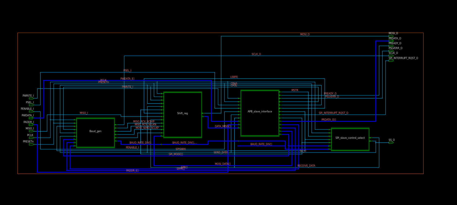
Why modular RTL?
Implementing the whole SPI protocol in a single block would make the design harder to understand, debug, verify and reuse.
A modular design separates the responsibilities:
- APB Slave Interface — communicates with the processor through APB, stores configuration and data, and provides status/interrupt information.
- Baud Rate Generator — creates SCLK timing and the event pulses used by the serial datapath.
- Shift Register — handles transmit and receive data shifting.
- SPI Slave Control Select — generates slave-select timing, counts the transfer and indicates completion.
This separation also makes it easier to inspect each block independently in simulation and synthesis.
7. Designing APB SLAVE INTERFACE
This module acts as the software-facing control block between the APB transaction interface and the SPI datapath.
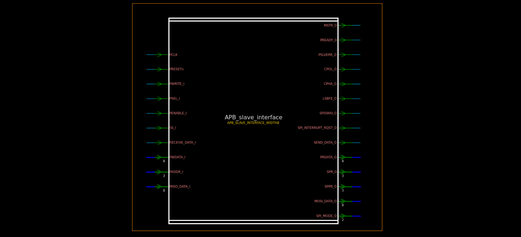
Behavioral functionalities :
- Detect APB
IDLE,SETUPandENABLEphases - Generate
PREADY_O - Generate the implemented
PSLVERR_Ocondition - Decode register addresses
- Handle register write and read operations
- Run SPI FSM and Store SPI configuration
- Provide transmit data to Shift register block
- Capture received data from Shift register block
- Generate status and interrupt information for the processor
Understanding the Behavioral Simulation
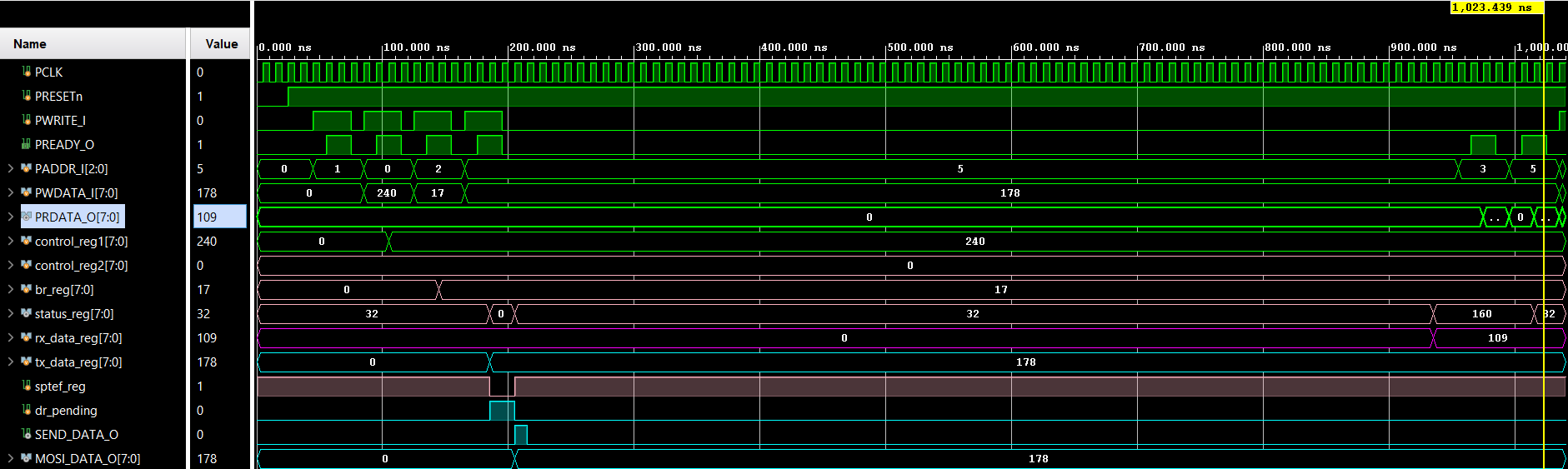
The behavioral simulation lets us follow how an APB transaction is converted into configuration and data inside the SPI controller.
The important sequence is:
-
APB writes the SPI configuration registers one by one.
The processor first writes the required control and baud-rate settings through the APB interface. -
The transmit data register is written with
178.
In the simulation, the APB master writes178(10110010) to the Data Register address (PADDR_I = 5). -
Transmit data and receive data are handled separately internally.
Although they are accessed through the same APB Data Register address, the implementation uses separate internal registers:tx_data_regfor transmitted data andrx_data_regfor received data. The former is written by the APB interface, while the latter is updated after an SPI transfer. -
Writing
tx_data_regclearsSPTEFand setsdr_pending.
SPTEFindicates that the transmit data register is empty. Once the processor writes new data,SPTEFbecomes0, whiledr_pendingbecomes1. This tells the controller that new transmit data is waiting to be transferred. -
The controller waits until the SPI datapath is ready to accept the new data.
When the APB interface is no longer writing the transmit register andSS_Iis high (meaning that no SPI transfer is currently active), the controller generates theSEND_DATA_Opulse. -
The transmit data is then passed to the Shift Register block.
During this transfer handoff,tx_data_regis presented throughMOSI_DATA_O, whileSEND_DATA_Oindicates that the Shift Register should load the new transmit data. -
The actual serial transmission happens inside the Shift Register block.
At this point, the APB interface has finished its job. The Shift Register takes the parallel transmit data and converts it into the serial SPI stream. -
The receive path works in the opposite direction.
After the SPI transfer completes, the data captured by the Shift Register is transferred intorx_data_reg. -
In the shown simulation,
rx_data_regbecomes109.
The received value is then available to the APB interface for software to read. -
Finally, the APB master reads the Data Register.
At the highlighted point in the waveform,PADDR_I = 5andPRDATA_O = 109, showing that the received SPI data has been successfully returned through the APB interface.
At this stage, we have only followed the control and data handoff between APB and the SPI datapath. The exact process of loading the transmit data, shifting individual bits, sampling MISO, and constructing the received value will become much clearer when we examine the SPI_SHIFT_REGISTER block in the next section. The high-level data path is:
APB write DR
      |
      v
Transmit data / pending state
      |
      v
SPI transfer
      |
      v
Received serial data
      |
      v
Receive register
      |
      v
APB read DR
A data-register write creates pending transmit activity. Once the SPI control logic allows the transfer to start, the transmit data is passed into the SPI datapath. After the serial transfer completes, received data is available for APB readback.
8. Designing BAUD GENERATOR
The BAUD_GENERATOR is the timing engine of the SPI datapath.
Its job is not simply to divide PCLK. It converts the programmable baud-rate settings into the SPI clock and generates the timing events that tell the Shift Register when to transmit and when to sample data.
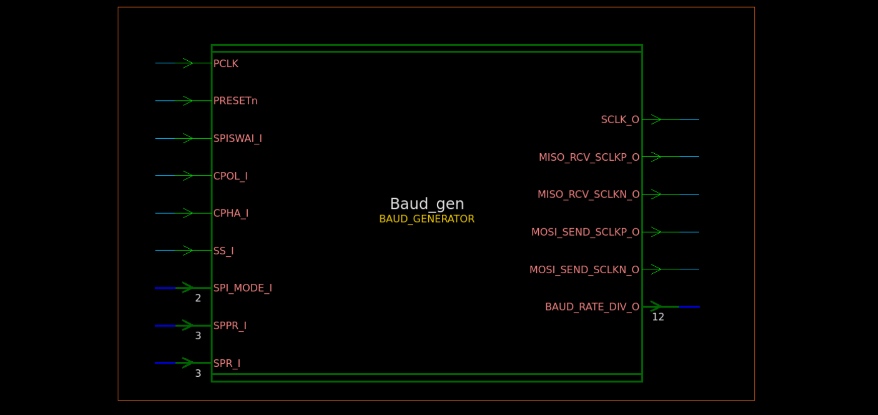
Behavioral functionalities
The Baud Generator performs three closely related tasks:
-
Calculate the SPI baud-rate divider.
The programmedSPPRandSPRvalues determine the active baud-rate division:BAUD_RATE_DIV = (SPPR + 1) × 2^(SPR + 1)This divider determines the relationship between the system clock
PCLKand the generated SPI clock:SCLK frequency = PCLK / BAUD_RATE_DIV -
Generate the SPI clock.
An internal counter countsPCLKcycles and togglesSCLKwhenever the half-period count is reached. Since the clock toggles twice during one complete SCLK period, the resulting SCLK period corresponds toBAUD_RATE_DIVsystem-clock cycles. -
Generate timing events for the Shift Register.
The Shift Register does not independently generate or derive the SPI timing. Instead, the Baud Generator provides four event pulses corresponding to the possible transmit and receive edges:MISO_RCV_SCLKP_O— receive/sample event associated with the rising edge ofSCLKMISO_RCV_SCLKN_O— receive/sample event associated with the falling edge ofSCLKMOSI_SEND_SCLKP_O— transmit/update event associated with the rising edge ofSCLKMOSI_SEND_SCLKN_O— transmit/update event associated with the falling edge ofSCLK
Which pair is active depends on the configured
CPOLandCPHAvalues.
Note:
SCLKis generated only whileSS_Iis asserted low and the SPI controller is operating in a mode where clock generation is enabled.
Why use a programmable divider?
The APB/system clock is normally much faster than the desired SPI serial clock. A programmable divider allows software to select the SPI transfer rate without changing the system clock.
This is particularly useful because the same SPI controller can communicate with peripherals requiring different serial-clock frequencies simply by changing the baud-rate configuration registers.
SCLK generation
The basic timing sequence inside the Baud Generator is:
       SPPR + SPR
           |
           v
    BAUD_RATE_DIV
           |
           v
      PCLK counter
           |
      half-period
        reached
           |
	   v
       SCLK toggles
           |
           v
    timing-event pulse
While the SPI interface is idle, SCLK is held at the configured CPOL level and the active baud-rate division value is prepared.
Once SS_I becomes low and clock generation is enabled, the counter begins counting PCLK cycles. When the half-period count is reached, SCLK toggles and the counter starts again.
In this way, the Baud Generator converts a much faster parallel system clock into the slower serial timing required by SPI.
Understanding the Behavioral Simulation
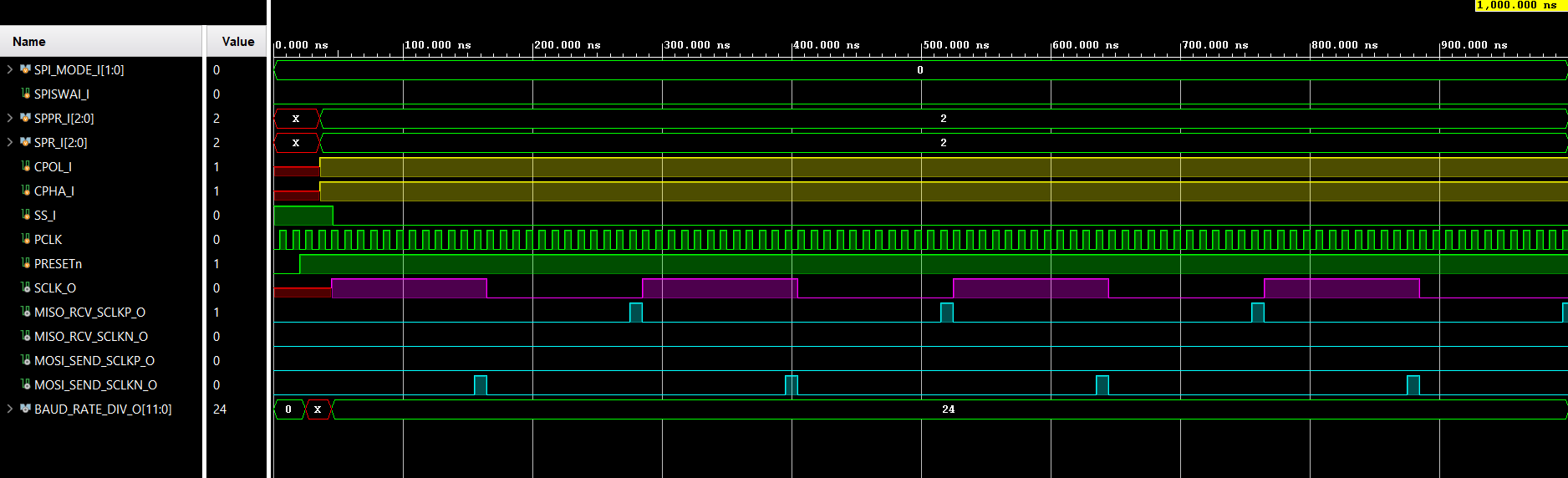
The simulation makes the relationship between SS_I, the baud-rate divider, SCLK, and the four timing events much easier to see.
The important observations are:
-
During the idle state,
SS_Iremains high.
The SPI transfer is inactive, soSCLKis held at its configured idle level determined byCPOL. The active baud-rate divider is also prepared during this state. -
The transfer begins when
SS_Ibecomes low.
Once the slave-select signal is asserted and the configured SPI mode allows clock generation, the internal counter begins countingPCLKcycles. -
The counter controls the SCLK transitions.
When the programmed half-period is reached,SCLKtoggles. Repeated counter cycles therefore generate the complete SPI clock waveform. -
The selected SPI mode determines which timing events are generated.
In this simulation,CPOL = 1andCPHA = 1. For this combination, the Baud Generator activates:MISO_RCV_SCLKP_OMOSI_SEND_SCLKN_O
These events correspond to the receive and transmit operations required for this SPI mode.
-
The timing events occur one
PCLKcycle before the corresponding SCLK transition.
This is an important detail of the implementation. The Baud Generator asserts the appropriate event pulse in advance, allowing the Shift Register logic to perform the required operation in coordination with the upcoming SCLK edge.
This one-cycle look-ahead is what allows the Shift Register to remain synchronized with the SPI timing without having to independently generate or monitor SCLK.
From clock generation to data movement
At this point, the role of the Baud Generator can be summarized as:
APB baud-rate configuration
            |
            v
     BAUD_RATE_DIV
            |
            v
       PCLK counter
            |
            +--------------> SCLK
            |
            +--------------> Timing events
                                  |
                                  v
                         SPI_SHIFT_REGISTER
The Baud Generator therefore forms the timing bridge between the system clock and the serial SPI datapath.
The next question is: what does the Shift Register actually do with these timing events?
The parallel transmit data (`178` in our example) is converted into serial `MOSI` bits, while incoming `MISO` bits are sampled and reconstructed into the received value (`109` in our example).
9. Designing SPI SHIFT REGISTER
The SPI SHIFT REGISTER forms the serial datapath of the controller. While the Baud Generator is responsible for when data moves, the Shift Register is responsible for what data moves.
It performs the actual parallel-to-serial transmission on MOSI and serial-to-parallel reception from MISO, one bit at a time.
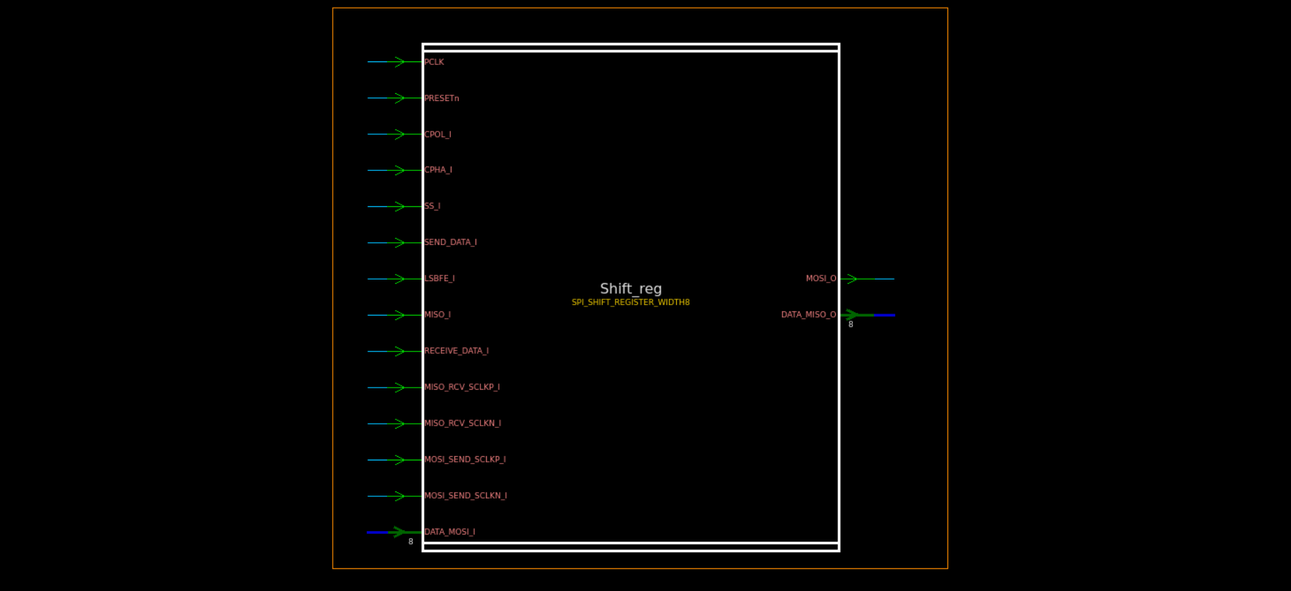
Behavioral Functionalities
The Shift Register contains two dedicated registers:
Tx_shift_reg— stores the transmit data and shifts it toward theMOSIoutput.Rx_shift_reg— collects the incomingMISObits and reconstructs the received parallel data.
For this implementation, WIDTH = 8, so both registers are 8 bits wide.
The fundamental operations are simple: shift the transmit register as each bit is sent, and shift each sampled MISO bit into the receive register.
if(bitcnt1 < WIDTH-1)
begin
    Tx_shift_reg <= Tx_shift_reg >> 1;
    bitcnt1      <= bitcnt1 + 1;
end

if(bitcnt2 < WIDTH)
begin
    Rx_shift_reg <= {MISO_I, Rx_shift_reg[WIDTH-1:1]};
    bitcnt2      <= bitcnt2 + 1;
end
The transmit register shifts right after a bit has been transferred, while the newly sampled MISO bit is inserted into the most-significant position of the receive register.
Implementation note: A shift-based approach is used here instead of variable bit indexing. This keeps the datapath simple and allows the synthesizer to map the operation directly onto standard shift-register hardware.
Connecting the Shift Register to the rest of the design
The Shift Register does not generate its own SPI timing. Instead, it receives the timing-event flags generated by the BAUD GENERATOR.
These flags indicate when the Shift Register should:
- update the transmitted
MOSIbit, and - sample the incoming
MISObit.
The transmit data originates from the APB_SLAVE_INTERFACE through DATA_MOSI_I. When SEND_DATA_I is asserted, the parallel APB data is loaded into Tx_shift_reg.
After the SPI transfer is complete, the accumulated value in Rx_shift_reg is returned to the APB interface through DATA_MISO_O when RECEIVE_DATA_I is asserted.
The resulting datapath is:
              APB SLAVE INTERFACE
                     |
              DATA_MOSI_I
                     |
                     v
              +--------------+
              | Tx_shift_reg |
              +--------------+
                     |
                     | serial
                     v
                    MOSI
                     |
                SPI transfer
                     |
                    MISO
                     |
                     v
              +--------------+
              | Rx_shift_reg |
              +--------------+
                     |
              DATA_MISO_O
                     |
                     v
              APB SLAVE INTERFACE
This makes the role of the Shift Register clear: the APB interface provides the parallel data, the Shift Register serializes and deserializes it, and the Baud Generator determines when each operation takes place.
Transmit Path
The transmit path converts the parallel value written through APB into a serial MOSI stream.
For our example:
APB data
  178
   |
   v
10110010
   |
   v
Tx_shift_reg
   |
   v
Serial MOSI bits
When SEND_DATA_I becomes active, the value 178 (10110010) is loaded into Tx_shift_reg.
For the configured SPI mode in this simulation, the transmit timing event is MOSI_SEND_SCLKN_I. Each time this event is asserted, the current transmit bit is presented on the serial datapath and the shift register advances to the next bit.
After all eight bits have been transferred, Tx_shift_reg has shifted through the complete word and reaches 0.
Receive Path
The receive path operates at the same time as transmission because SPI is inherently full-duplex.
On the receive event, the current value of MISO_I is sampled and inserted into Rx_shift_reg:
Rx_shift_reg <= {MISO_I, Rx_shift_reg[WIDTH-1:1]};
For the simulation shown below, the incoming bits progressively build the received value:
1 → 3 → 6 → 13 → 27 → 54 → 109
After eight received bits have been sampled, the final value becomes:
Rx_shift_reg = 109
Therefore, the same eight SCLK cycles that transmit the 178 value also receive the 109 value.
This simultaneous transmit-and-receive operation is the key characteristic of full-duplex SPI communication.
Understanding the Behavioral Simulation
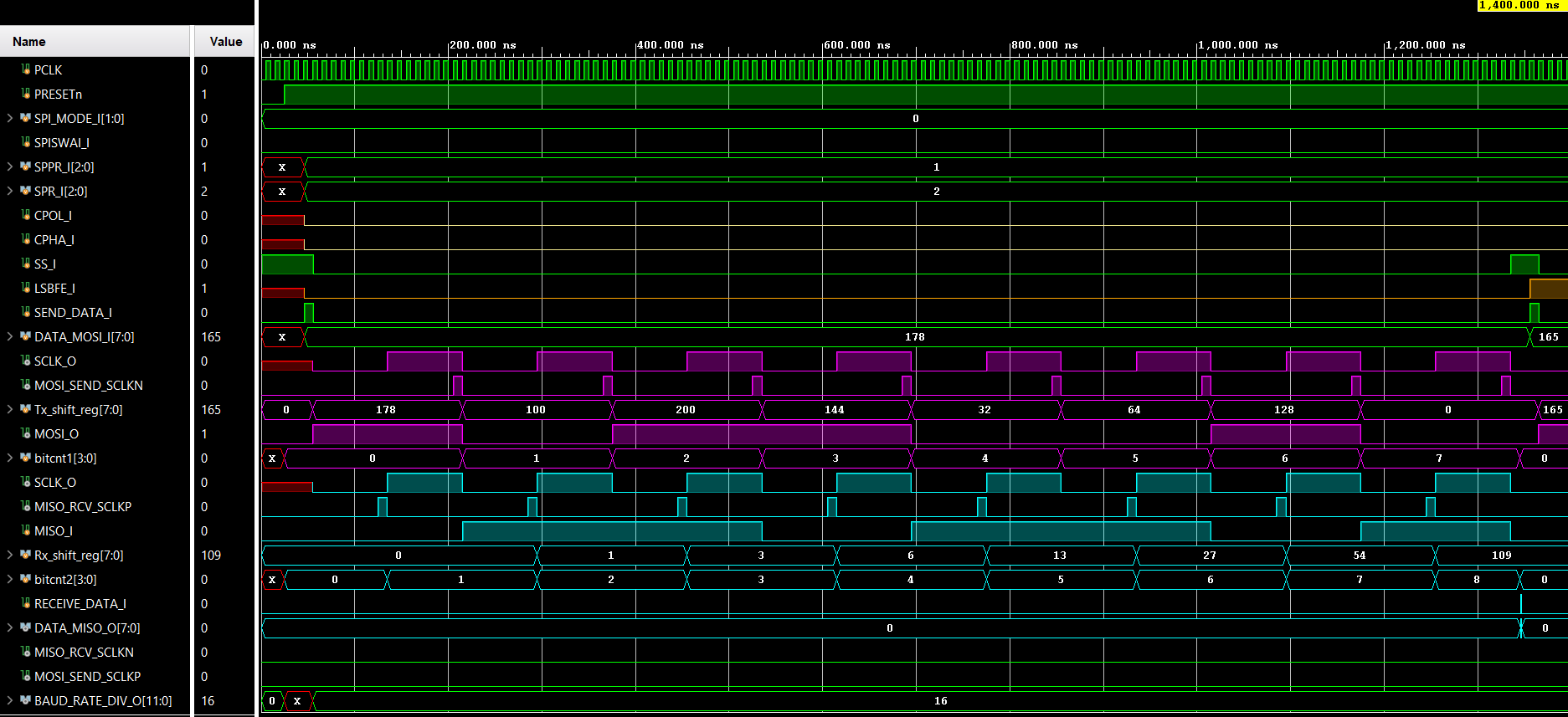
The waveform brings the interaction between the Baud Generator and Shift Register together.
The important sequence is:
-
Parallel data is loaded.
WhenSEND_DATA_I = 1, the transmit register is loaded withDATA_MOSI_I, which contains178(10110010). -
The slave-select signal becomes active.
WhenSS_Igoes low, the SPI clock begins toggling according to the programmed baud-rate settings. -
The Baud Generator produces timing events.
For theCPOL = 1,CPHA = 1configuration used in this simulation, the relevant events areMOSI_SEND_SCLKN_Ifor transmission andMISO_RCV_SCLKP_Ifor reception. -
Transmit and receive happen concurrently.
On the transmit event, the currentTx_shift_regbit is transferred towardMOSI. On the receive event, the currentMISO_Ivalue is sampled intoRx_shift_reg. -
The data moves one bit at a time.
Across eight SCLK cycles, the value178is transmitted while the incoming serial data is accumulated into the receive register. -
The transfer completes.
At the end of the eight-bit transfer,Tx_shift_reg = 0, indicating that all transmit bits have been shifted out, whileRx_shift_reg = 109, indicating that the complete eight-bit receive value has been assembled.
The simulation therefore demonstrates the complete serial datapath:
       178 = 10110010
              |
              v
        Tx_shift_reg
              |
              v
             MOSI
              |
        SPI full-duplex
              |
              v
             MISO
              |
              v
        Rx_shift_reg
              |
              v
           109 received
The important point is that the Shift Register does not need to know the overall transfer duration. It simply reacts to the timing events generated by the Baud Generator and performs the required transmit or receive operation at the appropriate point in the SPI cycle.
With the serial datapath now understood, the remaining question is: who controls the beginning and end of the SPI transfer?
That responsibility belongs to the SPI_SLAVE_CONTROL_SELECT block, which controls SS and determines when the SPI transfer starts and finishes.
…
10. Designing SPI SLAVE CONTROL SELECT
The SPI SLAVE CONTROL SELECT block is one of the smaller blocks in the SPI Master Controller, but it plays an important role in controlling the lifetime of an SPI transaction.
While the Baud Generator determines the timing of SCLK and the Shift Register handles the actual serial data movement, this block determines when the transfer starts, how long it remains active, and when the received data becomes available to the APB interface.
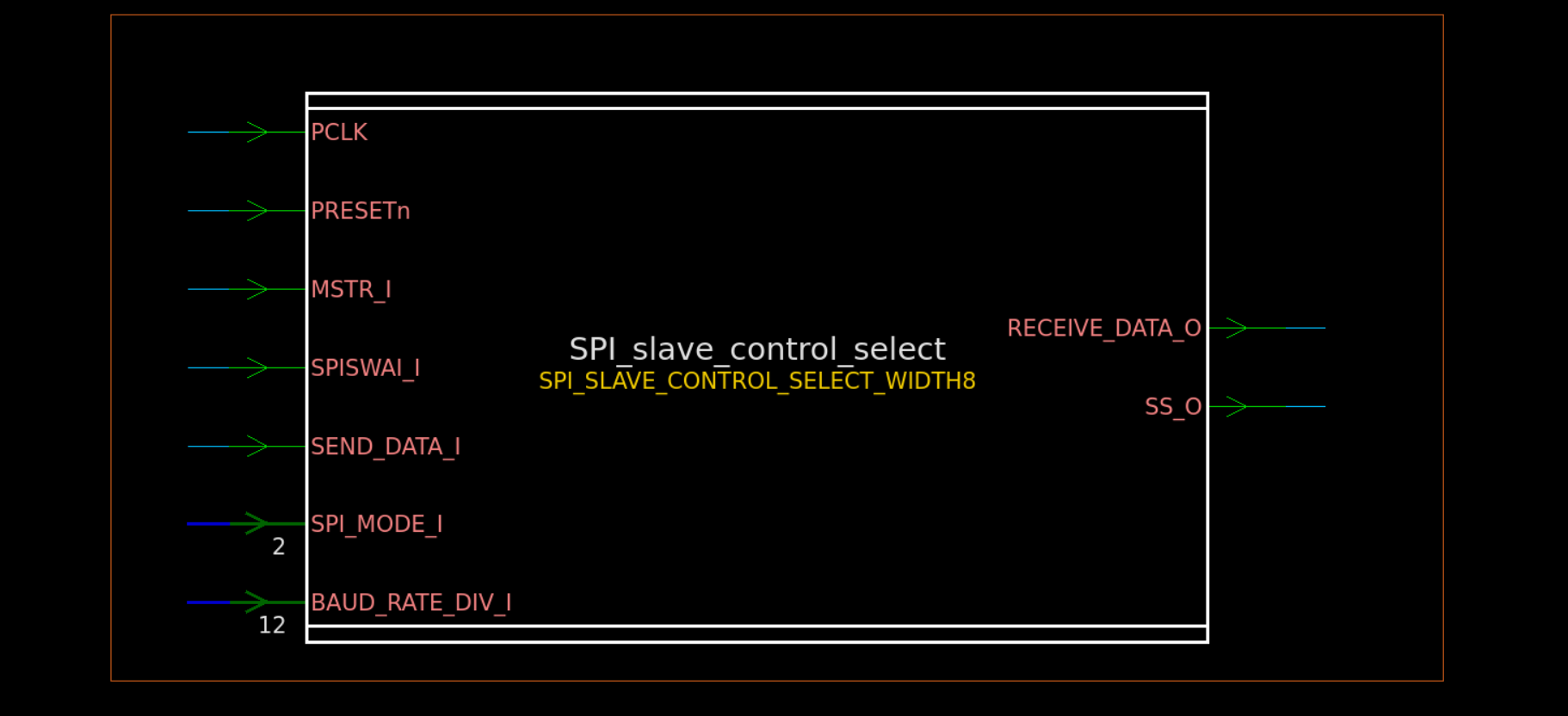
Behavioral Functionalities
The SPI SLAVE CONTROL SELECT block performs three main functions:
-
Controls the SPI transaction window.
It generates the active-lowSS_Osignal, determining when the selected SPI slave should begin and end a transaction. -
Controls the duration of the transfer.
Once a transfer begins, an internal counter tracks the number ofPCLKcycles required to transmit the complete frame. This ensures thatSS_Oremains asserted for the required number of SCLK cycles. -
Signals when received data is available.
After the complete frame has been transferred, the block assertsRECEIVE_DATA_O, allowing the received value from the Shift Register to be passed back to the APB interface throughDATA_MISO_O.
The high-level sequence is:
SEND_DATA
    |
    v
SS asserted low
    |
    v
SCLK active
    |
    v
Count transfer duration
    |
    v
Transfer complete
    |
    v
SS deasserted high
    |
    v
RX data available
This makes the block the transaction-level controller of the SPI datapath.
Determining the Transfer Duration
The duration of an SPI frame depends on two quantities:
- The number of
PCLKcycles represented by one complete SCLK period, given byBAUD_RATE_DIV_I. - The number of bits in the SPI frame, given by
WIDTH.
The current RTL calculates the maximum transfer count as:
wire [15:0] MAX = BAUD_RATE_DIV_I << logb2(WIDTH);
For the current 8-bit configuration:
WIDTH = 8
log2(8) = 3
Therefore:
MAX = BAUD_RATE_DIV_I << 3
    = BAUD_RATE_DIV_I × 8
For example, when:
BAUD_RATE_DIV_I = 8
WIDTH           = 8
the resulting transfer count is:
MAX = 8 × 8 = 64 PCLK cycles
This corresponds to an eight-bit SPI frame, because one complete SCLK period occupies eight PCLK cycles.
Implementation note: The shift operation is effectively a multiplication by
2^log2(WIDTH)for power-of-two frame widths such as 8 bits. This implementation therefore directly expresses the relationship between the baud-rate division and the number of bits in the transfer.
Understanding the Behavioral Simulation
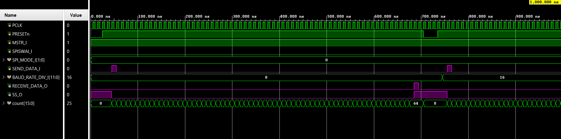
The simulation shows how the block controls the complete SPI transaction.
In this simulation:
WIDTH           = 8
BAUD_RATE_DIV_I = 8
MAX             = 64
The important sequence is:
-
The transfer begins when
SEND_DATAis asserted.
The controller activates the slave-select signal, drivingSS_Olow. -
The SPI clock becomes active.
WithSS_Oasserted, the Baud Generator produces the requiredSCLKwaveform. -
The transfer counter starts tracking the frame.
The counter advances with the system clock while the SPI transfer is active. -
The counter reaches 64.
SinceMAX = 64, the controller keeps the slave selected for the 64PCLKcycles required for the complete eight-bit transfer. -
The transaction ends.
Once the required transfer duration has elapsed,SS_Ois deasserted and returns high. -
Received data becomes available.
At the completion of the frame,RECEIVE_DATA_Ois asserted, indicating that the received value can now be transferred from the Shift Register to the APB interface.
The relationship can be visualized as:
BAUD_RATE_DIV = 8
        |
        v
  8 PCLK cycles
  per SCLK period
        |
        v
   8 SCLK periods
   for 8-bit frame
        |
        v
   64 PCLK cycles
   total transfer
        |
        v
  SS_O deasserts
        |
        v
 RECEIVE_DATA_O = 1
Thus, the Slave Select Control block provides the boundary around the serial transaction: assert SS, allow the required number of SCLK cycles to occur, terminate the transaction, and indicate that the received data is ready.
With the individual functional blocks now understood — APB interface, Baud Generator, Shift Register, and Slave Select Control — the next step is to bring everything together.
That is where SPI_TOP becomes important: it connects these blocks into a single working SPI Master Controller and allows us to observe the complete transaction from an APB write all the way to the final APB read.
…
11. Top-Level Integration: SPI TOP
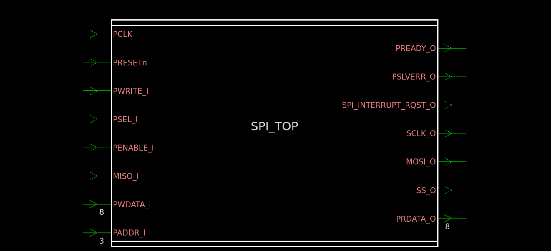
SPI_TOP instantiates:
APB SLAVE_INTERFACE
BAUD GENERATOR
SPI SHIFT REGISTER
SPI SLAVE CONTROL SELECT
and connects the configuration, timing, datapath and transfer-control signals.
External interface
The top level exposes the APB control/data interface together with the serial SPI interface.
| Group | Signals |
|---|---|
| APB clock/reset | PCLK, PRESETn |
| APB control | PWRITE_I, PSEL_I, PENABLE_I, PADDR_I |
| APB data | PWDATA_I, PRDATA_O |
| APB response | PREADY_O, PSLVERR_O |
| SPI | SCLK_O, MOSI_O, MISO_I, SS_O |
| Interrupt | SPI_INTERRUPT_RQST_O |
The top-level module is intentionally simple: its main job is to instantiate the four functional blocks and connect their internal interfaces.
12. Building the Testbench
The verification environment should answer one basic question:
If software writes transmit data, does the controller actually produce the expected SPI transfer and return the expected received data?
The representative transaction used in this project is:
APB WRITE
TX = 178
   |
   v
SPI TRANSFER
   |
   v
RX = 109
   |
   v
APB READ
RX = 109
The testbench configures the controller through APB, writes the transmit data, allows the SPI transfer to execute, drives serial data on MISO, and then reads the received result back through APB.
The waveform shown in the next section is the integrated top-level simulation view from Vivado.
13. Understanding the Final Simulation Waveform
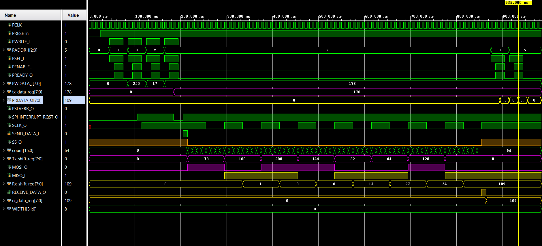
The final top-level waveform combines the bus-level and SPI-level behavior.
APB side
Follow:
PCLKPRESETnPWRITE_IPADDR_IPSEL_IPENABLE_IPREADY_OPWDATA_IPRDATA_O
SPI control
Then follow:
SS_OSCLK_OSEND_DATA_I
Serial datapath
Finally inspect:
MOSI_OMISO_ITx_shift_regRx_shift_regRECEIVE_DATA_Orx_data_reg
What happens in the shown transfer?
- The APB side writes
178into the transmit path. - The controller asserts
SS. SCLKbegins toggling.- The transmit shift register drives the serial MOSI data.
- MISO is sampled during the transfer.
- The receive shift register evolves through the observed values:
1 → 3 → 6 → 13 → 27 → 54 → 109. - The transfer completes and
SSreturns inactive. - The received value becomes available to the APB side.
- The APB read returns
109.
So the complete software-to-serial-to-software path is:
178
  |
  v
SPI serial transfer
  |
  v
109
  |
  v
APB readback
The important verification point is not just that a final number appears. The waveform shows the interaction between APB phases, slave-select, SCLK, serial data, and the internal shift registers.
14. RTL Linting and Design Checks
Simulation can tell us whether the tested transaction behaves as expected. Lint and design checks examine the RTL from a structural and implementation-oriented perspective.
Typical checks can include:
- Unused signals
- Width mismatches
- Undriven signals
- Unconnected ports
- Coding constructs that can produce unintended hardware
During cleanup, the unused declarations:
reg Tx_status, Rx_status;
in SPI SHIFT REGISTER were removed because they were assigned but not used elsewhere.
The remaining design-check messages led to a useful debugging exercise around the baud-rate divider.
15. A Real Synthesis Debugging Moment
During the Design Compiler flow, the design-check report contained messages around:
BAUD_RATE_DIV[0]
Specifically, the remaining messages indicated that this bit was not connected to internal logic and that the corresponding hierarchical input/output bit had no effective load.
Initial reaction
Everything had looked fine in simulation. Then check_design produced a message around one bit of the baud-rate divider. The natural first question was: did a real connection get lost?
Trace the RTL
The divider is calculated as:
BAUD_RATE_DIV = (SPPR + 1) × 2^(SPR + 1)
The key observation is:
2^(SPR + 1)
is always even.
Therefore:
BAUD_RATE_DIV[0] = 0
for every possible SPR value in this implementation.
That means the least-significant bit of the divider cannot carry information. Synthesis can therefore optimize away logic associated with that redundant bit.
The design-check messages were:
LINT-28:
BAUD_GENERATOR.BAUD_RATE_DIV_O[0] is not connected to any nets.

LINT-28:
SPI_SLAVE_CONTROL_SELECT_WIDTH8.BAUD_RATE_DIV_I[0]
is not connected to any nets.

LINT-60:
Hierarchical pin BAUD_RATE_DIV_I[0] has no internal loads.
The important lesson is that a structural warning is not automatically a functional failure. The right response is to trace the signal, understand the RTL mathematically, and then decide whether a functional change is actually required.
16. From RTL to Gates: Synthesis
Now we move from behavioral RTL to an implementation mapped to a target technology library.
The synthesis flow used in this project was:
Verilog RTL
    |
    v
Analyze
    |
    v
Elaborate
    |
    v
Link
    |
    v
Compile
    |
    v
Mapped netlist
Tool:
Synopsys Design Compiler
T-2022.03-SP4
Target library:
lsi_10k.db
A synthesis tool takes the RTL description, elaborates it into hardware structures, optimizes the logic, and maps the resulting design to cells from the target library.
The key point is that the synthesized circuit is an implementation of the RTL under a specific set of timing and library assumptions.
17. Timing Analysis
The synthesis flow used a 20 ns clock period:
create_clock -name clk -period 20 [get_ports PCLK]
set_input_delay 0.75 -clock clk [get_ports [all_inputs]]
set_output_delay 0.75 -clock clk [get_ports [all_outputs]]
A 20 ns period corresponds to a nominal 50 MHz clock target.
The reported values were:
| Timing metric | Result |
|---|---|
| Clock period | 20 ns |
| Data arrival time | 17.26 ns |
| Data required time | 19.15 ns |
| Slack | +1.89 ns |
What does +1.89 ns mean?
For the reported path, the data arrived before the required timing point, leaving a positive margin of 1.89 ns.
A useful mental model is:
Available timing window
0 ns -------------------------- 20 ns

Actual path
0 ns ----------------- 17.26 ns

Remaining margin
17.26 ns -------- 19.15 ns
                    <--->
                    1.89 ns
The exact setup path and endpoint should still be read from the complete timing.rpt; the table above summarizes the reported values retained from this project.
18. Area Analysis
Reported synthesis summary:
| Metric | Result |
|---|---|
| Ports | 172 |
| Nets | 998 |
| Cells | 783 |
| Combinational cells | 645 |
| Sequential cells | 134 |
| Buffer/Inverter cells | 74 |
| Combinational area | 1014 |
| Non-combinational area | 1190 |
| Total mapped cell area | 2204 |
2204is the mapped cell area reported by synthesis. It is not a physical chip-area result including interconnect.
The report also notes that physical total area was not available because no wire-load model was specified.
The area number is therefore best interpreted as a technology-mapped cell-area figure for the synthesis run, not as the die area of a finished chip.
19. Power Analysis
Reported synthesis estimate:
| Metric | Result |
|---|---|
| Cell internal power | 0.0000 nW |
| Net switching power | 1.0848 µW |
| Reported switching/dynamic estimate | 1.0848 µW |
| Leakage | 0 |
The power report also contains the library characterization warning PWR-799.
Therefore:
1.0848 µW should be presented as the available switching-power estimate from the synthesis report, not as a fully characterized physical total-power figure.
This distinction matters because library characterization and activity information determine how meaningful a synthesis-time power estimate is.
20. What Did the RTL Become?
The transformation can be viewed conceptually as:
RTL abstraction
      |
      v
Logic optimization
      |
      v
Technology mapping
      |
      v
Synthesized gate/cell netlist
The synthesized netlist represents the implementation selected by the synthesis tool for the chosen target library and constraints.
It is useful for inspecting:
- Which library cells implement the RTL
- How the logical design was mapped
- What structural form the synthesized controller takes
- Which logic may have been optimized away
It does not, by itself, represent a completed physical layout with routing, placement, clock-tree implementation, parasitics and final sign-off results.
21. What I Learned
This project changed the way I look at RTL.
Simulation is necessary, but it is not the finish line. A design can behave correctly in the tested simulation and still produce useful warnings once it is elaborated and synthesized.
One of the most useful lessons was learning not to “fix” a warning immediately. The BAUD_RATE_DIV[0] case looked suspicious at first, but tracing the arithmetic showed why the bit was redundant.
The project also reinforced the value of modular RTL. Keeping the APB interface, baud generator, shift register and transfer-control logic separate made the design easier to reason about and easier to debug.
Finally, timing, area and power are not just numbers at the end of a project. They are part of understanding what the RTL turns into.
22. Complete Design Flow
The entire project can be summarized as:
Specification
     |
     v
SPI + APB architecture
     |
     v
Modular Verilog RTL
     |
     v
Vivado simulation
     |
     v
RTL lint / design checks
     |
     v
Design Compiler synthesis
     |
     +---- Timing
     +---- Area
     +---- Power
     |
     v
Synthesized netlist
This is the complete path from protocol requirements to an analyzed technology-mapped implementation.
23. Source Code and Project Files
The complete implementation is available on GitHub:
APB-Based SPI Master Controller
The project contains the RTL, simulation material, documentation, lint/synthesis scripts, reports and synthesized netlist selected for the repository.
Source-of-truth note: The Verilog RTL is authoritative for the exact behavior of the current implementation. This article explains the implementation and the observed tool results; it does not replace the RTL.
24. What’s Next?
The next article in the series will move from a bus/peripheral controller to another fundamental RTL structure:
Designing an Efficient Synthesizable FIFO in Verilog
Later, the series will build toward:
Synchronous FIFO
    ↓
Asynchronous FIFO / CDC
    ↓
AXI4-Lite → APB Bridge
    ↓
FPGA CNN Accelerators
    ↓
Latency / Throughput / BRAM / DSP Optimization
The larger goal is to keep connecting RTL architecture with verification, synthesis and implementation trade-offs.